This time, I outline S-85M0A and S-85M1A, ultra-high efficiency step-down switching regulators. I have introduced S-85S1P which has supply voltage divided output function to monitor battery voltage before in No.3 and No.4. New S-85M0A and S-85M1A apply WLP (Wafer Level Package) which involves packaging the die while it is still on the wafer, no bonding wires for connecting and as a result, they have become very small, thin and more suitable for wearables and IoT devices. Table 1 shows a comparison of mounting area between S-85M0A and international and domestic competing products whose inductors are integrated into the modules. S-85M0A is a product using an inductor as an external component. But you may find that it realizes greater reduction of the size and thinness in total area including external parts. The coil is an external component of the S-85M0A or S-85M1A. So ABLIC says that even thinner coil can be supported according to the customer's request, in addition to the thinness of the IC.
| S-85M0A | Company A | Company B | Company C | |
| IC size | 2.0 × 1.6 × 1.0 (mm) |
2.9 × 2.3 × 1.1 (mm) |
2.0 × 2.5 × 1.04 (mm) |
|
| Total area including external parts (note) | 2.7 × 1.6 = 4.3 mm2 |
2.6 × 2.5 = 6.5 mm2 |
2.9 × 2.3 = 6.7 mm2 |
3.5 × 2.9 = 10.2 mm2 |
Note: S-85M0A is using an inductor as an external component.
Inductors in other products are integrated into the modules.
Table 1. Product comparison (Mounting area)
One more feature of the S-85M0A and S-85M1A is low EMI (Electro-Magnetic Interference).
By using WLP package, EMI caused by bonding wires is eliminated. Figure 1 shows the measurement result of the magnetic field distribution near the S-85M0A Demo Board. The results suggest that electromagnetic noise decreases as frequency increases. In the range of 800MHz – 1GHz, EMI is lower than 300MHz – 800MHz and in the 1GHz – 2GHz, EMI is further reduced. From these results, S-85M0A and S-85M1A are expected to provide low noise capability in applications which use frequency band around the 1-2GHz such as Sub-1GHz for LPWAN and over 1GHz band for GPS signal.

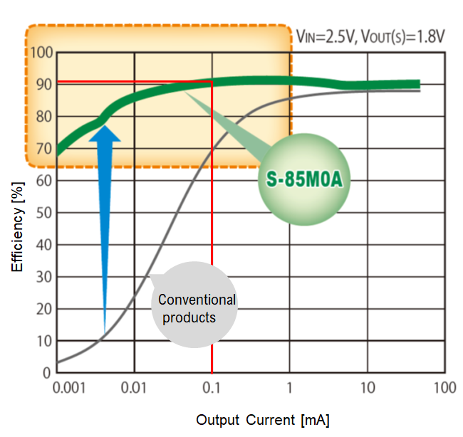
With regards to the quiescent current, S-85M0A and S-85M1A support the same quiescent current 260nA as S-85S1P and this is the industry's top-level value. Looking at the efficiency, the orange-colored box in the Figure 2 shows that efficiency is improved remarkably than previous products at light loads of 1mA or less. Efficiency value is 90.5% at 100uA load as the solid red line shows and it strongly supports a long battery life of the devices.

In this way, S-85M0A and S-85M1A reduce their size and thickness and realize industry's most compact package. In the process, WLP package technology is adopted and it makes it possible to suppress EMI emission minimally in the medium and higher frequency bands where the range is commonly used for IoT devices. In addition to these features, with ultra-low current consumption and high efficiency, the Power Management ICs S-85M0A and S-85M1A provide essential elements to various IoT markets where further growth can be expected.
In the next article, I shall consider the ways to deliver these regulators to customers, to IoT device development scene more quickly.
Related Information
- [News Release] ABLIC Inc. launches the S-85M0A Series of ultra-high efficiency step-down switching regulators in the industry's most compact (*) size
- [Product information/Datasheet] Step-down Switching Regulator S-85M0A Series
- [Product information/Datasheet] Step-down Switching Regulator S-85M1A Series